Felix Ortiz: Hey — rough question to start, are you a person who thinks Moore's Law is dead or a person who thinks it's fine?
Tess Hollis: Oh, I think that question is the problem, actually.
Felix Ortiz: See, that's — yeah, that's sort of where I landed too, but let me give you the number first because it reframes everything. TSMC and Intel call their newest chips '2nm' and '3nm.' The actual gate width on those transistors is 40 to 50 nanometers. Not two. Forty to fifty.
Tess Hollis: Hold on — so the label and the physical dimension aren't even in the same order of magnitude.
Felix Ortiz: Not even close. And the thing is — that's not a secret. Engineers know this, analysts know this. It's just that the language got decoupled from the measurement and nobody... called the moment.
Tess Hollis: Okay, so name what that actually means. Gordon Moore's 1965 paper was a prediction about transistor density — a specific, countable, physical thing. For five decades you could look at a node name and it pointed at a real dimension. Now it doesn't. So the industry has quietly stopped tracking the quantity that Moore's Law is actually about.
Felix Ortiz: And here's what I don't know — is that because the physics made it impossible to keep going, or is it because it got too expensive and inconvenient and specialization was more profitable? Because one of those is physics saying no, and the other is business saying 'not worth it.' Those are really different.
Tess Hollis: That's the whole episode right there.
Felix Ortiz: Moore's Law dead as physics. Dead as a business model. Or — and this is the one I find weirdest — still technically alive but measuring something it never used to measure. I came in thinking I knew which answer was right and I genuinely don't anymore.
Tess Hollis: And the naming lie is what surfaces it. Because as long as chips are still called '2nm,' everyone can keep acting like the old story is intact.
Felix Ortiz: Which means the question isn't just about transistors — it's about whether the whole framing of 'progress' in compute still means what we think it means.
Tess Hollis: And the framing question is the right one to sit with — but before we can answer whether it's physics or business, we have to be clear on what the physics actually is. Because I think most people have a fuzzy version of it.
Felix Ortiz: Yeah, okay — what's the plain version?
Tess Hollis: Imagine a light switch. You make it smaller and smaller until the wall it's embedded in is only a few atoms thick. At that point, electrons don't wait for the switch to open. They just pass straight through the wall. That's quantum tunneling, and it is not a solvable engineering problem. It's physics saying the switch doesn't work anymore.
Felix Ortiz: Oh — wait. So it's not that the switch breaks. It's that the concept of 'off' stops being meaningful.
Tess Hollis: Exactly that. And the threshold is around one nanometer of gate-oxide thickness. Below that, tunneling leakage current is so significant you can't tell whether a transistor is on or off reliably. Gordon Moore's original 1965 observation worked for fifty years because you could just keep shrinking the geometry on a flat plane — planar MOSFETs — and you got density, speed, and cost efficiency more or less for free.
Felix Ortiz: Right — so the weird part is it worked *so* consistently for so long that people kind of forgot there was a physical object underneath the trend line.
Tess Hollis: And here's where it actually gets more broken than the tunneling story alone. Dennard scaling — the companion principle, the part that said smaller transistors also use proportionally less power — that snapped around 2005, 2006. Leakage currents just stopped cooperating. So the density gains kept coming for another decade, but you were no longer getting the power efficiency for free.
Felix Ortiz: Hold on — 2005? That's way earlier than I would have said.
Tess Hollis: Yeah. The clock speed wall — CPUs stopped getting faster around that same period. That was the symptom. Dennard scaling collapsing was the mechanism.
Felix Ortiz: Okay and then — actually, no, let me get this straight — FinFETs and gate-all-around transistors, GAAFETs, those are already in production chips today. Not demos. Shipping silicon. And the idea was they'd fix the electrostatic control problem at sub-10nm. But even with that geometry fix — wrapping the gate around three or four sides of the channel — we're still hitting the wall?
Tess Hollis: Still hitting it. Because the transistor geometry problem and the quantum tunneling problem are not the same problem. GAAFET helps with leakage from poor gate control. It does not help with electrons that quantum-tunnel through the oxide itself. Those are separate physics.
Felix Ortiz: So we already solved — or partially solved — the geometry problem, and the wall is still there. That's the part that should unsettle people.
Tess Hollis: And the lithography side compounds it. To pattern features below ten nanometers you need EUV — extreme ultraviolet light — because you literally cannot resolve features smaller than your light's wavelength. That equipment costs hundreds of millions of dollars per machine. So even before the physics ends you, the cost of chasing it might. Which is what makes the 'physics or business' question so hard to answer cleanly.
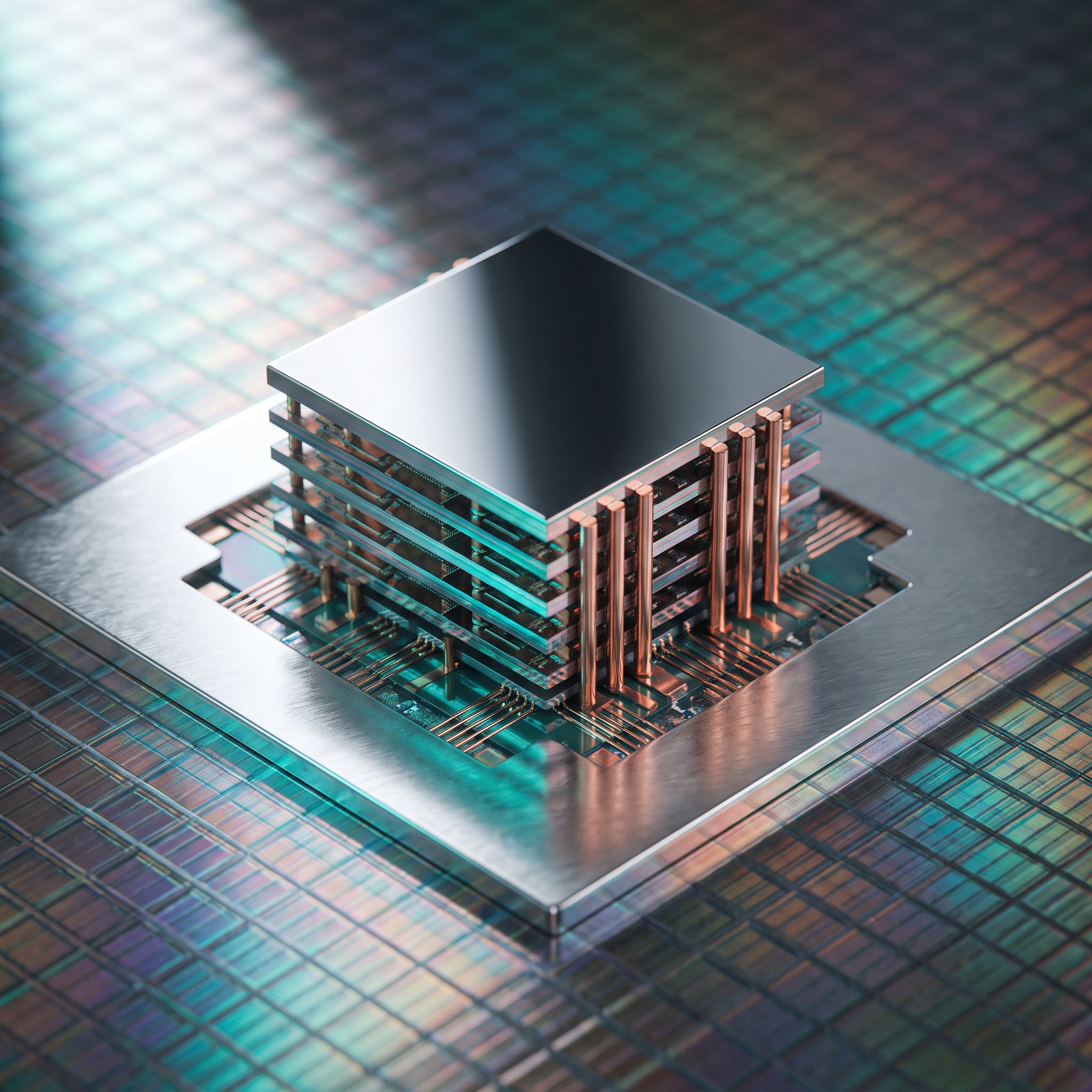
Felix Ortiz: And that cost problem is actually what pushed the whole industry vertical. Like, literally vertical — if you can't shrink the plane, you stack the plane. That's the logic behind what TSMC, Samsung, and Intel are all pouring R&D into right now. 3D ICs, chiplets on interposers — you get density gains through packaging, not through transistor shrinkage.
Tess Hollis: Wait — so AMD's chiplet architecture is the commercial proof of concept here?
Felix Ortiz: Yeah, that's the clearest example shipping at scale. You disaggregate the monolithic chip — instead of one big die, you've got smaller independent chiplets, each optimized for a specific function, different process nodes, better yield because a defect kills a small chiplet instead of the whole thing. And then you integrate them on a shared interposer in 2.5D, or stack them fully vertical in 3D.
Tess Hollis: Okay, but here's what nobody names cleanly. You solve the area problem by compacting compute into a smaller volume — and what does that do to heat?
Felix Ortiz: It makes it worse. Right? You've — wait, actually this is the part that genuinely surprised me when I dug into it — you've relocated the constraint, not removed it. Same heat, smaller volume to move it out of.
Tess Hollis: The thermal constraint that stopped horizontal scaling is now a vertical problem. And cooling infrastructure is designed for flat chips.
Felix Ortiz: Right — so the industry is winning tactically while the wall gets closer in a different dimension.
Tess Hollis: And this lands in concrete places. A biotech startup's ML team runs inference on NVIDIA H100s. New architecture drops next quarter — physically incompatible. Porting the pipeline takes six engineers four weeks. Do they upgrade?
Felix Ortiz: For most companies that math just doesn't work. Only the trillion-dollar cloud providers absorb that without blinking.
Tess Hollis: And the chiplet model makes this more frequent, not less. More architecture fragmentation, more incompatibility cycles. The cost is real — it just doesn't show up on the chip spec sheet.
Felix Ortiz: Yeah and — okay, there's a version of this where carbon nanotube transistors, CNTFETs, eventually give you a 3D-native material with better thermal properties. But that's a candidate, not a product. Manufacturing at scale is still a hard open problem.
Tess Hollis: So we're sitting in the gap between the tactical win and the unsolved constraint.
Felix Ortiz: Which — and we'll get to this — is exactly what makes the specialization turn so contested. Whether GPUs and TPUs are the answer because physics demanded it, or because it was just more profitable to go that route first. That's a different argument than heat.
Tess Hollis: But the specialization story — okay, that's the part I want to pin down, because the way it usually gets told is backwards. People say physics broke, therefore GPUs and TPUs. But NVIDIA wasn't sitting around waiting for a physics emergency. They just decided to own matrix math completely and walk away from general-purpose.
Felix Ortiz: Right — and that's a strategy call, not a physics inevitability. Intel was still trying to be everything to everyone and NVIDIA just... didn't.
Tess Hollis: So what's the version nobody says out loud? The fragmentation happened because specialization was profitable first. The physics constraint made it defensible later.
Felix Ortiz: Yeah and — okay, this is what actually gets me. Google built TPUs specifically for AI inference and training. Not because CPUs couldn't do it. Because the cost-per-operation math on custom silicon was just better. That's a business decision with a physics costume on.
Tess Hollis: Wait — so now you've got NVIDIA owning AI training on the GPU side, AMD chasing them, Google with TPUs, neuromorphic chips for entirely different workload classes. That's not a solution. That's a portfolio of bets.
Felix Ortiz: And Huawei pursuing multi-layer scaling on their own track because they're cut off from the leading-edge nodes anyway. So the fragmentation is geopolitical too, not just architectural.
Tess Hollis: Okay, but here's the asymmetry that nobody names. The trillion-dollar cloud companies — Google, the ones building TPUs — they absorb the software porting cost when architectures become incompatible. A mid-size team doesn't have six engineers to spend four weeks rewriting a pipeline.
Felix Ortiz: Oh — wait, so the specialization era actually concentrates compute advantage at the top. Like, the fragmentation isn't neutral, it has a winner built in.
Tess Hollis: The cost is real, it just doesn't appear on a chip spec sheet. It shows up in engineering hours and migration risk. Everyone outside the big cloud providers pays it — they just don't call it a Moore's Law consequence.
Felix Ortiz: Okay and then — actually, no, this is what gets weird to me. AI-assisted design automation gets proposed as the answer. The idea being you extract Moore's Law-equivalent gains from design-space exploration instead of physical shrinkage. But is that actually continuing Moore's Law or is it just... redefining 'doubling' to mean whatever we can currently achieve?
Tess Hollis: That's the question. Gordon Moore's 1965 observation was about a measurable physical quantity. If 'doubling' now means 'AI found a better floorplan,' you've changed the unit.
Felix Ortiz: And FinFETs and GAAFETs are already in production silicon — not demos, shipping chips — and the doubling rate still isn't recovering. So the geometry problem got partially solved and we're still hitting the wall. That's — I mean, that's the hardest fact here. We already did the transistor geometry fix and it wasn't enough.
Tess Hollis: So the question isn't whether we can engineer around the physics anymore. It's whether redefining progress is a continuation of Moore's Law or a eulogy for it written in optimistic language.
Felix Ortiz: Yeah and — I keep wanting to land on an answer and I just... can't. Because what actually happened is TSMC, Samsung, Intel — they're all pushing 3D integration hard. NVIDIA owns AI training. AMD has the chiplet playbook. Google has TPUs. And none of those things talk to each other the way CPUs used to talk to everything. It's not a successor. It's just — a bunch of separate bets that each solve a different slice of the problem.
Tess Hollis: That's the thing that actually unsettles me. The old story was unified — Gordon Moore's 1965 observation worked because one metric, transistor density, pulled everything else with it. Faster CPU meant faster everything. Now the stack is fragmented by design. And that's not a bug. That's the architecture.
Felix Ortiz: Right — and what replaced it requires strategy.
Tess Hollis: Not just time. Strategy. Which means the compounding gains that felt like a law of nature — where your laptop just got better every two years without anyone deciding anything — that's gone.
Felix Ortiz: And the open question — the one I actually can't answer — is whether the software, the economics, the human expertise to navigate this fragmentation, whether any of that can keep pace. Like, can enough teams actually manage a world where NVIDIA, AMD, and Google TPUs all require different optimization strategies?
Tess Hollis: Nobody knows yet.
Felix Ortiz: Nobody knows yet. I think that's — actually, no, I think that's the most honest place we've landed. I came in thinking this was a 'Moore's Law is dead' conversation and it turned out to be a 'nobody's agreed on what replaces it' conversation. Which is weirder.
Tess Hollis: Weirder and more interesting. Thanks for sitting in it with me.